
Samsung Foundry has submitted paperwork with authorities in Arizona, New York, and Texas looking for to construct a foremost-edge semiconductor manufacturing facility in the USA. The prospective fab near Austin, Texas, is predicted to expense above $17 billion and to make 1,800 work. If anything goes as planned, it will go on line by the fourth quarter of 2023. There is an intrigue about the new fab although: Samsung hasn’t mentioned which method node it will be made for. Could Samsung be the to start with to 3nm in the Usa?
Samsung Foundry to Expand in the United states of america
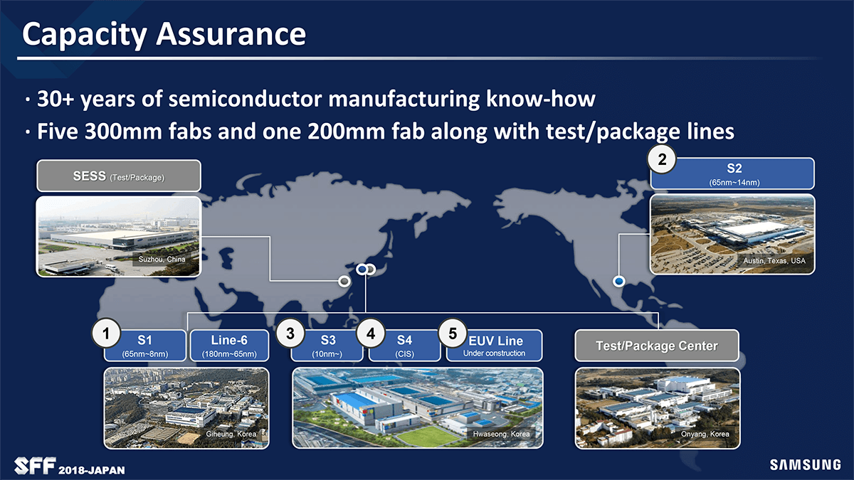
As demand from customers for semiconductors is rising, Samsung Foundry and other makers of chips are expanding their production capacities. In the latest many years the business built chips applying its major-edge producing technologies exclusively in South Korea, while its S2 producing facility in Austin, Texas, was still left with 14LPP (and derivatives down to 11LPP) and more mature fabrication processes that are way too outdated for major edge goods. When it comes to chip style and design, Samsung has plenty of customers within the US (these as IBM, Nvidia, Qualcomm, Tesla, just to name a handful of) that need to use its most advanced nodes and would favor to use fabs located in the Usa, which is why it desires to develop a new production facility in this state. Moreover, the organization also requires a new foremost-edge fab in North The usa to better contend from its rival TSMC, which programs to develop a semiconductor generation facility in Arizona by 2024.
Samsung Foundry formally started to check out options to create a new fab in Arizona, New York, and Texas a short while ago, according to Austin American-Statesman. The recent system submitted to the governing administration of Texas consists of a 7 million square ft (650 thousand sq. meters) facility on the firm’s 640-acre web site (i.e., the fab will be adjacent to the existing S2) that will charge in excess of $17 billion. The business has no options to upgrade the S2 in the foreseeable future as mature method technologies are nevertheless demanded by its consumers.
Exhibiting the current S2 fab
There are 4 criteria that the new site have to meet in a bid to make perception for Samsung’s major-edge fab, according to the files submitted with the Texas authorities: entry to expertise, current semiconductor manufacturing ecosystem, pace to market place, and robust public- personal partnership (i.e., incentives). Samsung presently has a fab in Texas, so it already has expertise and a provider ecosystem in the state. By contrast, it will have to struggle both equally for expertise and supplies in Arizona (in opposition to Intel and TSMC) and New York (towards GlobalFoundries).
To develop a major-edge producing facility, Samsung demands rather huge incentives from authorities. In unique, Samsung is requesting put together tax abatements of $805.5 million above 20 many years from Travis County and the metropolis of Austin, according to Reuters, which effectively signifies that Samsung needs a 100% tax abatement from the county and 50% from the metropolis. In addition, Samsung is in search of $252.9 million in tax breaks from the Manor university district based on the Texas Tax Code that lets residence tax breaks for financial development projects. So much, no company has acquired a 100% tax abatement wherever in the Usa, in accordance to market observers. However, the deal however will make a good deal of sense for the condition, and there is probable heading to be fascination from the federal govt as nicely.

“As there are other extremely aggressive marketplaces in search of to get this expansion deal, it is imperative that our point out and nearby governments perform alongside one another to guarantee Austin arrives out on major,” mentioned Amber Gunst, CEO of the Austin Technological know-how Council. “Not only does this deliver 1,800 employment that will be readily available to Central Texans of all training and skill degrees, this expansion makes an even more powerful marriage amongst Samsung and Austin, a romantic relationship we price immensely.”

Samsung expects the new fab to have an financial output of all-around $8.642 billion and salaries for long lasting personnel to full $7.323 billion in the very first 20 decades of its operation.
Task Silicon Silver: Coming On line in Q4 2023
The programs for the new fab are named Undertaking Silicon Silver (PSS), and it will be positioned adjacent to S2. It will not use any of the current properties of S2, but will be a fully new fab created from the floor up. It will have its very own operations support, central utility setting up, industrial waste procedure, air separation plans, storage for inert gases, and other constructions.

“The only at present-contemplated interconnections concerning the new facility and the bordering current residence might be a pedestrian and/or substance bridge or walkway made amongst the current improvements on the web page and the new building,” the doc submitted to the authorities reads.

Samsung will devote $5.069 billion on buildings and genuine estate assets improvements as very well as $9.931 billion in semiconductor producing devices.
Samsung Foundry does not disclose numerous information about the new fab. At present, we know that if the enterprise symptoms all vital papers with the authorities in Austin, it will split ground by Q2 of 2021 with the expectation that manufacturing will be up and jogging by Q4 of 2023. In addition, we also know that the facility will occupy 650 thousand square meters of land. To place that amount into context, TSMC’s Fab 18 in Tainan (in the Southern Taiwan Science Park) will occupy 950 thousand sq. meters of land when it is thoroughly designed. In standard, Samsung is preparing to create a fairly enormous manufacturing facility. TSMC’s Fab 18 has a objective of 120k-140k wafer starts for every month at whole quantity, so we really should anticipate PSS to be all-around the 70k-100k mark assuming similar specifications and scaling.
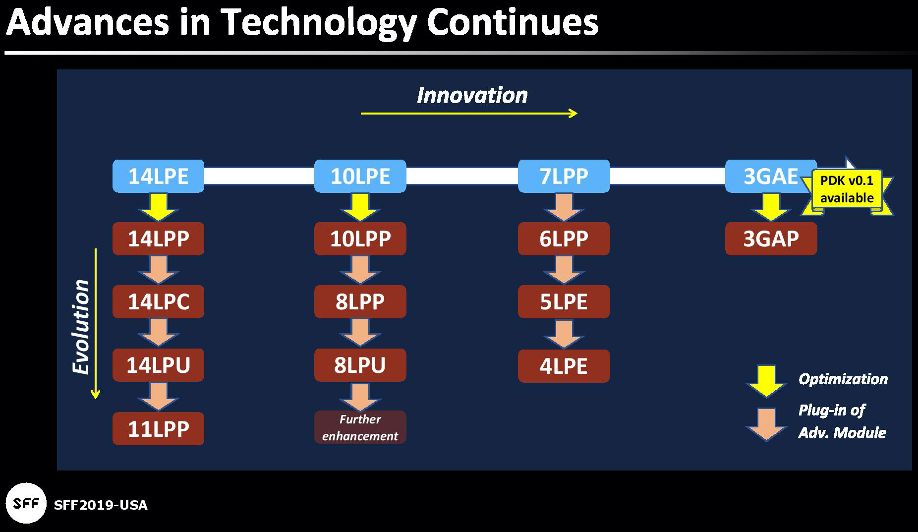
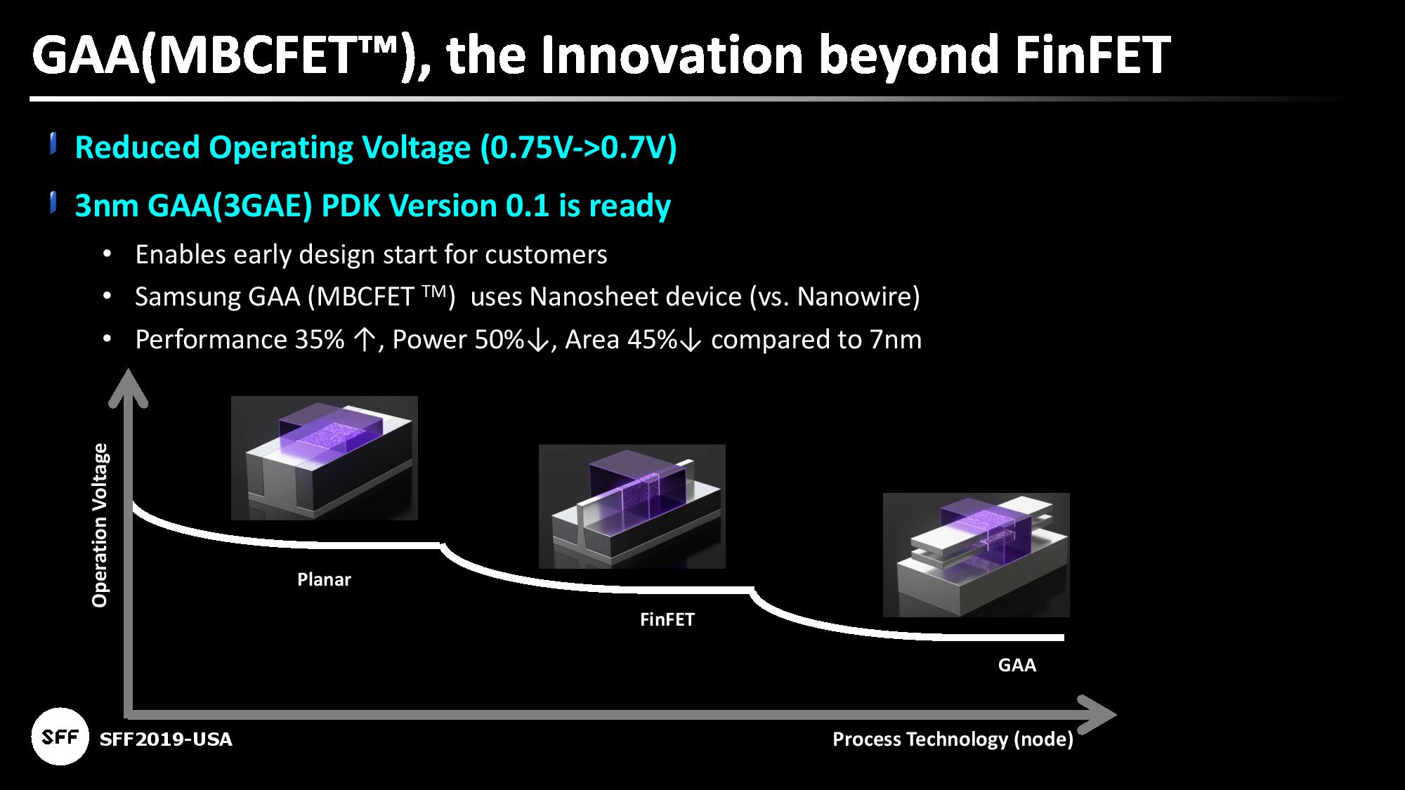
Samsung Foundry does not disclose which method systems it plans to use at the new fab, but it is risk-free to say that they will use extreme ultraviolet (EUV) lithography. Considering the point that Samsung expects its 3 nm technology based mostly on gate-all-close to (GAA) multi-bridge channel area outcome transistors (MBCFETs) to be completely ready in 2021 ~ 2022 timeframe, it is rational to be expecting it to be utilised at the fab together with other technologies. In the stop, Samsung’s V1 fab in South Korea will be utilized for multiple nodes, together with 3 nm.
Centered on at present available info, Samsung is preparing a bigger undertaking than its rival TSMC. TSMC’s planned fab in Arizona will have an preliminary generation ability goal of about 20,000 wafer starts for each month (WSPM) and will hire 1,600 persons immediately. TSMC intends to shell out $12 billion on its new fab from 2021 to 2029, which suggests that TSMC’s new fab will be a more compact facility when compared to the new Samsung fab in Texas.
No R&D Pursuits, Manufacturing Only
The files that Samsung has submitted to the authorities clearly suggest that the Challenge Silicon Silver is a purely manufacturing facility and the firm does not strategy to run any R&D pursuits there.
Considering that there will be no analysis and growth performed at the new fab, Samsung Foundry will not be ready to apply for any kind of United states of america govt assist when it comes to semiconductors R&D even just after correct plans will be handed by the legislators.
Furthermore, Samsung’s S2 fab does not have the Usa Division of Defense’s Trusted Foundry position, so it does not glimpse like the company would make any chips for the DoD. In fact, it is unclear whether it is fascinated in armed forces contracts in the United states in common.
Summary
After GlobalFoundries pulled out from creating leading-edge process systems in 2018 and Intel shed its method technologies direct to TSMC and Samsung Foundry, the United states government has been extra ready to support local chipmakers in a bid to guarantee that the country is self-reliant and does not rely on chips generated elsewhere.
TSMC was the initially to get advantage of the Usa willingness to support community semiconductor generation and its $12 billion fab in Arizona will commence production of chips utilizing its N5 node (and likely N5P and N4 derivatives) in 2024. Meanwhile, TSMC’s fab in Arizona with an first 20,000 WSPM potential will not be as huge as the services it has in Taiwan. To serve the United states of america authorities orders, TSMC’s facility will have to obtain the Trusted Foundry position, if/the moment it receives it, it will be able to offer authorities chips created using a pretty state-of-the-art node. In addition to TSMC, some of its suppliers are also gearing up to make new facilities in the United states.
Samsung Foundry, the world’s second greatest agreement maker of chips, is one more foundry to establish a primary-edge fab in the United states The company’s Challenge Silicon Silver production facility in Texas will cost in excess of $17 billion and is projected to be larger when in contrast to TSMC’s fab in Arizona. It stays to be noticed which course of action know-how SF options to use at the fab, but a person of the selections is its 3 nm MBCFET-primarily based foremost-edge node. In the meantime, it is unclear whether Samsung is seeking to construct chips for the Usa govt organizations.
Although the Usa govt would prefer to enable area chipmakers, this kind of as Intel or GlobalFoundries, its initiatives to assist creation of chips in the region have so far gathered sizeable desire from Taiwan-centered TSMC and South Korea-based Samsung. In any circumstance, it appears like the strategy to carry main-edge semiconductor production again to the Usa functions and a $27 million planned expense is a superior evidence of that, dependent on tax abatements all through the method.
Linked Reading through: